As Doped Monocrystals
Benefits related with our arsenic doped crystals
General product specification
Brief product description
Arsenic doped silicon crystals present a sophisticated semiconductor product used in electronics.
The crystals are produced from very pure raw materials and intentionally highly doped with the Arsenic. Production process objective is to prepare the best material base for excellent final devices with superior parameters and functionality.
The crystals are sliced to wafers and act mainly as a substrate used within a production of Epitaxial wafers.
The wafers are intended for a production of discrete semiconductor devices.
In a consumer market stage the discrete devices are used especially in the automotive industry, communications, and information technologies.
Our As doped Monocrystals can provide you the following benefits:
- Excellent electro-physical parameters,
- Customized / Tailor-made production,
- Superior electronic grade inputs (Hemlock, Wacker, Momentive, SGL,…),
- High value for competitive price,
- Careful services (possibility of grounding, flatting, transportation, superior packing,...).
General product specification
Many key crystal parameters influence in different ways the quality and the functionality of a specific resulting device. Thus, the arsenic doped crystal specifications vary, based on customers needs, very often. Due to the specific parameter needs, the crystals are considered as special and customized products.
Our actual As doped monocrystal production possibilities are presented by the following general arsenic doped crystal specification.


Here you can download PDF version:


| No. | Parameter | Unit | Value | Remark |
| 1 | Production method | - | CZ |
|
| 2 | Diameter | mm | 4", 5", 6" | Caliper |
| 3 | Orientation | - /deg | (111) ±1,0 | ASTM F26 |
| (100) ±1,0 | ||||
| 4 | Conductivity type | --- | N | ASTM F42 |
| 5 | Dopant | --- | Arsenic | Purity 6N |
| 6 | Resistivity (centerpoint) | Ωcm | < 0,005 | ASTM F84 |
| < 0,003 | ||||
| 7 | Radial resistivity variation | % | <25 (111) | ASTM F81 - PLAN B |
| < 10 (100) | ||||
| 8 | Oxygen content | ppma | to bee determined |
|
| 9 | Carbon content | ppma | < 0,5 | SIMS; see point 24 |
| 10 | Boron content | at.cm-3 | < 1*E14 | ASTM F1528; see p. 24 |
| 11 | Dislocation density | cm-2 | < 100 | ASTM F1725 |
| 12 | O.S.F. | cm-2 | < 100 | ASTM F1727 |
| 13 | Primary flat-length | mm | to be determined | ASTM F671 |
| 14 | Primary flat-orient. | - /deg | to be determined | ASTM F847 |
| 15 | Length limitation | mm | to be determined |
|
| 20 | Crystallographic perfection: Free from grain boundaries, twin boundaries, swirls, slip lines and lineages. | |||
| 21 | Mechanical damage: Free from visually observed cracks, scratches, blowholes, chips and contamination. | |||
| 22 | Crystal ingot form: Ground (Ra< 1.5) or "as grown" surface. Edge of the front plane ground to max. distance 1 mm. Deflection of the front plane max. 2 mm. | |||
| 23 | Oxygen content is guaranteed by process capability. | |||
| 24 | Residual impurities (C, B, P, metals) are guaranteed by usage of virgin polycrystalline silicon Hemlock or Wacker. | |||
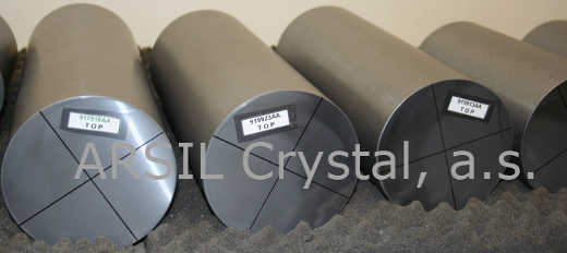
| 25 | Marking: „Y“ + „TOP“ and ingot number on the seed end. | |||
| 26 | Label: Manufacturer, Spec. no, Ingot no., Conductivity, Dopant, Orientation, Resistivity (spec.), Diameter (spec.), Length, Weight, Production date, Oxygen. | |||
| 27 | Packaging: Corrugated paper, transport case. | |||
| 40 | Note: THE PARAMATERS CAN BE CHANGED UPON REQUESTS OF CUSTOMERS. | |||